This is my first attempt at building a "proper" amplifier
for general use, as opposed to the Mixer-Amplifier I had made earlier. This amp
was made without too much concern to cost, hence several of the approaches I've
taken may be sub-optimal from the cost perspective.
Overview
Microcontroller-controlled preamplifier, with infrared remote control
capability. Volume and other settings stored in battery-backed RAM.
LCD Display for volume, etc.
Three general-purpose line-level inputs, one tape input, one tape output.
70W MOSFET-based stereo power amplifier.
Headphone output.
+/-38V at 4A and +/-5V at 500mA power supplies.
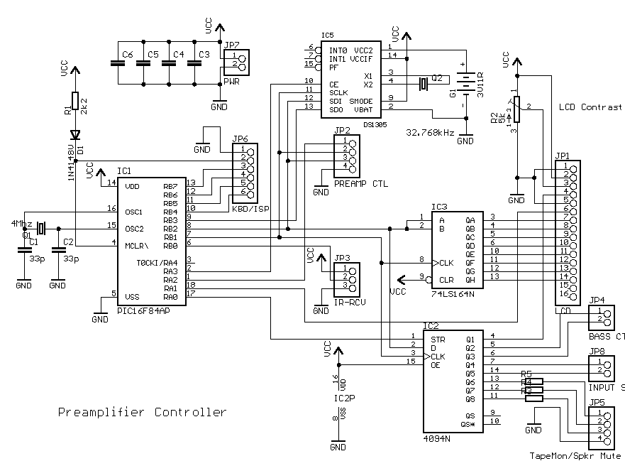
Microcontroller Unit (MCU)
This forms the central control secion of the amplifier. It
is based on a PIC16F84A microcontroller from Microchip. The microcontroller is
connected to the following peripherals:
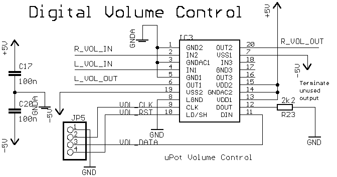
LM1973 μPot digital audio attenuator.
DS1302 real-time clock (RTC).
2x16 character mode LCD through a 74HC163 shift register.
CD4094 latched shift register, acting as general purpose output ports.
These ports are connected to CD4052 analog multiplexers which funcion as input
source selectors, tape monitor selectors and Bass Boost mode selectors. It's
also connected to the LCD panel's register-select pin and the speaker muting
relay driver.
TSOP1736 IR receiver module.
Three-button keypad.
Headphone socket swtch, used to indicate to the MCU that headphones are
plugged in, and to mute the main speakers.
The 16F84 is cheap, fast and has just the right amount of
memory for the task. It does not have enough I/O ports for all functions in this
application, hence I had to use serial "port extenders": using shift registers
to store data sent out over an SPI-Bus style interface. SPI bus needs to be used
anyway, to communicate with the RTC and the μPots.
MOSFET Integrated Amp Controller Circuit
Connector JP2 goes to the μPot on the preamplifier board.
The LCD connects through a standard Berg header. Some modules have a 2x8
connector in place of a 1x16, I'm not sure of the pinouts.
The 16F84 runs off a 4MHz crystal, so it can execute roughly
1 million instructions per second: more than enough for the task. It has 1k of
internal Flash program memory, 64 bytes EEPROM and 68 bytes RAM. The software is
written in the 16F84's assembly language, assembled with MPLAB and downloaded to
the target through a home-made 16F84 programmer. The keyboard port, connected to
RB7-RB4 is also used as the in-systep programming (ISP) port. To do this, the
MCLR pin is also brought out to the connector. The only disadvantage with this
is that programming for the keypad was difficult; you have to remove the
programmer and re-connect the keypad before you could test the new changes. The
software (.ASM file) is in the file preamp_ctl.zip
(9kB, version 1.3). I've tried to comment parts of the code, but it's not
complete. The code currently has no known bugs.
I originally intended the speaker muting relay and tape
monitor ports to go to three general-purpose LEDs, hence the series resistors.
They might, however, be a good idea, especially with the μPot connection, as it
will serve to increase risetime, and reduce the signal coupling between the
audio signals and the digital control signals.
The DS1305 RTC has a 32 kHz timekeeping crystal. It's main
use is for it's 96 bytes of battery-backed NVRAM, which are used to store the
current volume, input source and bass-boost selections, even when the power is
removed. I could have used the PIC's EEPROM for this, but it has a limited
number of write cycles. I'd either have to have a brown-out detection circuit
trigger an interrupt to make the PIC write to EEPROM, or live with a
limited-lifetime amplifier. Using NVRAM is easier. The MCU talks to the RTC
through an SPI bus (SCLK, SDI and SDO pins). The DS1305 includes a programmable
trickle-charger which can be configured through the SPI bus.
IC2 is a CD4094 shift register and latch. Data from the MCU
is clocked in serially through the D and CLK pins. When the strobe pin STR
receives a rising edge, the data from the shift register is internally latched
and fed to the outputs. This ensures that the outputs do not change state when
the MCU clocks data into or out of any of the other devices on the SPI bus (RTC,
μPot, etc). IC3 is an 8-bit SIPO shift register. It behaves like the 4094, but
there is no latch. This is because its outputs drive the LCD module, which has
an internal latch.
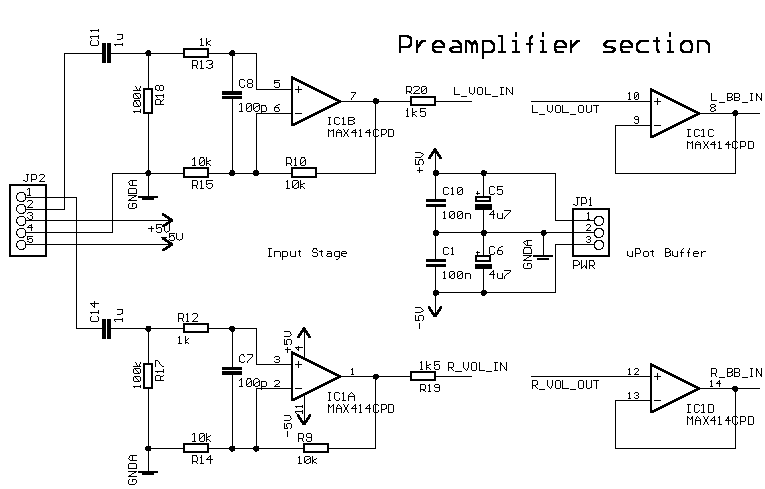
Preamplifier
The Preamplifier section uses an opamp-based circuit to
provide a total of +6dB gain, Volume control and two-step Bass Boost. Opamps
used are the MAX414 low voltage, low-noise opamps.
MOSFET Integrated Amp Preamplifier Input stage.
The first stage (IC1A and IC1B) uses a non-inverting
amplifier configuration. Looking at the channel based on IC1B, R13 and C8
provide RF suppresion, C11 and R8 behave as an LPF, and sets the input impedance
of the preamp at 100k. R10 and R15 set the gain of this stage at 2 (6dB). C1,
C5, C6 and C10 provide supply bypassing. Mount C1 and C10 near the IC.
In addition to the input stage, this diagram includes a pair
of buffers (IC1C and IC1D) used at the output of the μPot, which has a high
output impedance.
MOSFET Integrated Amp μPot
The LM1973 μPot is the digital volume control chip used in
this project. It contains three digitally adjustable audio attenuators with a
78dB adjustment range, and > 100dB mute. It accepts settings changes via an
SPI-bus compatible interface. In the circuit, JP5 connects to JP2 on the
controller board. It has one distinct advantage over similar devices made by
Dallas Semiconductor, etc. in that it uses a split supply. Thus, no exta
coupling capacitors are needed to interface these to opamps.
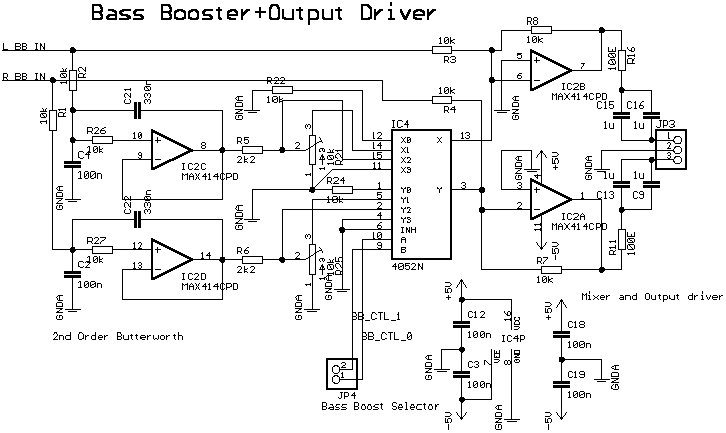
MOSFET Integrated Amp Bass Boost and Driver
The Bass Boost section provides two switchable levels of
Bass enhancement. The input audio is first low-pass filtered by a second-order
LPF, whose cutoff frequency is 100Hz. The LPF is built around IC2C and IC2DThe
output of the LPF is given to a MUX based on a CD4052. This mux can choose
between ground, an attenuated version of the LPF, and the full LPF output. The
selected MUX output is summed with the original audio, yeilding a Bass Boosted
signal. The outputs of this section are fed to the final power stage.
The trimpots R21 and R25 are used to set the bass level for
the low-bass mode. This is usually not just the midpoint (50%) level, it's
somewhere like 70%. It can be adjusted to personal taste. IC2A and IC2B act as
the summing amplifier and output stage driver. 100Ω resistors R11 and R16 are
used to prevent the load capacitance from causing instability in IC2A and IC2B.
2μF coupling capacitance is provided.
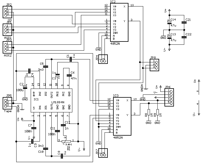
Input Selector
MOSFET Integrated Amp Input Selector
The Input Selector is built around two CD4052 analog
multiplexers. IC2 is used to select the input source (CD/AUX1/AUX2) and IC3 is
used to choose either the source selected above, the tape monitor or the tape
monitor after noise reduction using National Semiconductor's LM1894 Dynamic
Noise Reduction (DNR) chip. The DNR section is built around IC1, and is
discussed on this
page. JP1-3 are the source inputs, JP5 is the tape monitor input. R1 adjusts
the DNR level. This is adjusted while listening to a soft passage to just above
the point where the quietest part of the programme material "drops out". JP4 and
JP7 come from the MCU board and are used to select the inputs and tape monitor.
JP8 is the tape-out port, and has the currently selected input. It is not
buffered, but it should be. JP6 is the connection to the preamp board (both
power and signal). 1MΩ resistors are provided to ensure that the input
capacitors of the preamp do not cause popping when inputs are switched from one
source to the other.
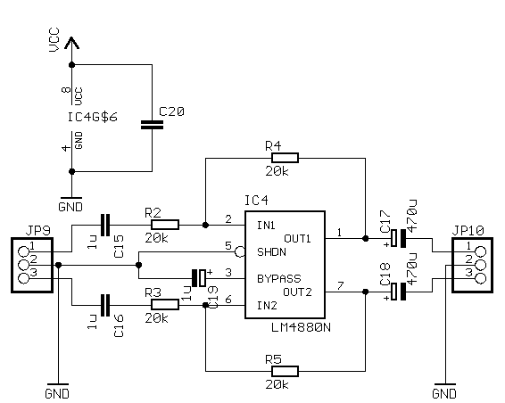
Headphone Amplifier
MOSFET Integrated Amp Headphone Amplifier
The headphone amplifier is based on National Semiconductor's
LM4880 headphone amplifier chip. It reduces the size of the headphone amp
used.
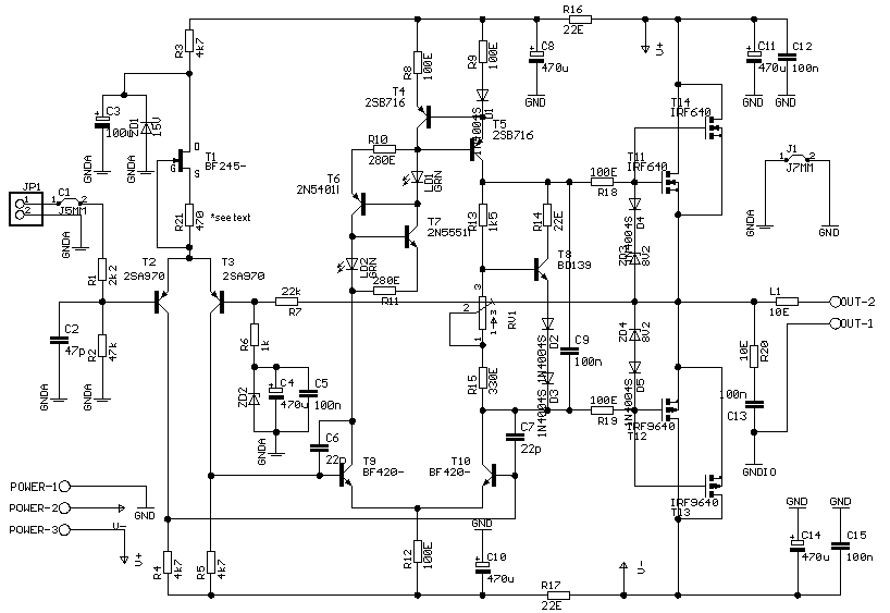
Power Amplifier
MOSFET Integrated Amp Power Amplifier
This circuit is from David White's article in Electronics
World (August 2001). It uses inexpensive HexFet™ Power MOSFETs as output
devices. Since their transconductance is low, the rest of the design is geared
towards producing maximum open-loop gain. Overall Negative Feedback is used to
set the gain to 27dB and to reduce the distortion.
The input devices used (2SA970) are low-noise, high gain PNP
devices. They have poor Vce(max), so their supply voltage is reduced
using a simple Zener diode regulator built using R3, ZD1 and C3. T1 is used as a
current source. The author of the original EW article mentioned using a plain
gate-source connected JFET, which is selected to produce 1mA current. At Rs. 25
a pop, I was not about to do this with BF245s. Besides, the current for my G-S
connected BF245s is around 7mA. Insert a resistance in series with the source to
reduce the current. Since the source-drain current is dependent on the
manufacturing process, you should select the resistor for each BF245 in a
multiple-amp. system. The value should be selected for 1mA current. If required,
use a 1k pot here.
C1 forms the input blocking cap, but is shorted with a
jumper because the blocking capacitor is already present on the preamp board. R1
and R2, together with C2 form an RF suppression network at the input. R2 sets
the input impedance at 47kΩ. R4 and R5 are the collector loads for T2 and T3. I
found that using a current mirror did not improve the THD rating of the amp (at
least in Spice), so I dropped that idea. ZD2 (A 2.7V Zener), C4 and C5 prevent
the base of T4 from getting beyond 2.7V in the event of amplifier clipping,
output device failure, etc.
T9 and T10 forms the voltage amplifer stage (VAS). The
original circuit recommended using 2SD756 transistors, which I couldn't find.
The BF420 is similar, with slightly lower beta. It's a differential stage, with
a constant current source formed by T6, T7, LD1, LD2, R10 and R11. A Wilson
current mirror, formed by T4, T5, D1, R8 and R9 acts as the collector load for
T9 and T10, ensuring maximum gain. T8, R13-15, RV1 D2 and D3 form the voltage
offset between the gates of the output devices, to bias them into Class AB
operation. RV1 sets the bias current. T8 should be in thermal contact with the
output devices. R10 and R19 are used to limit the current drawn by the gate
capacitance of the output devices. C6 and C7 form the Miller capacitors.
Remember that you will need to change this if any of the transistors are
substituted with different ones. I used styroflex capacitors here. R16, R17, C8
and C10 act as LPFs to filter the supply to the VAS and input stage.
D4, D5, ZD3 and ZD4 form a rudimentary short circuit
protection for the output MOSFETs. It will limit the current long enough for the
supply fuses to blow. C11, C12, C14 and C15 are supply decoupling capacitors.
C12 anc C15 should be placed near the MOSFET drains. C13 and R20 form the Zobel
network, used to compensate for the speaker coil's rising impedance with
frequency. L1 is a 10 ohm, 1W resistor with around 10 turns of enamelled wire
wrapped around it, connected in parallel. This is used to prevent the speaker
cable capacitance from causing amplifier instability. The circuit shown uses two
paralleled MOSFETS, although this is not required; it just gives addiional
stability. It may be necessary to insert 0.1 or 0.22 ohm 5W resistors in series
with each source before paralleling the MOSFETs, to prevent current
hogging.
R7 and R6 form the feedback network. These set the gain at
27dB. If oscillation is a problem, R7 can be bypassed with a 100pF or so
capacitor.
Note the separation of the signal and power grounds in the
circuit. The input stage is referenced to the signal ground GNDA. The decoupling
capacitors on the supply current are referenced to the power ground (GND). Also
note that the output Zobel network is referenced to a third ground labeled
GNDIO. GNDIO must be connected to the speaker connection posts' ground
terminals, which are then wired directly to the power supply via a thick ground
lead. A jumper is provided between GNDA and GND. I found that this jumper had to
be cut to give hum-free operation, but your configuration may yield different
results.
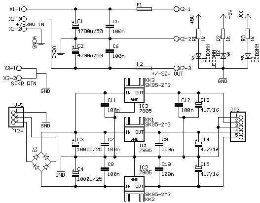
Power Supply
The power supply for the amplifier has two sections: the
low-voltage and high voltage sections. The high voltage section produces an
unregulated +/- 38V for the power amplifier. The low voltage section provides
+/- 5V for the analog sections (preamp, input selector, etc.) and +5V for the
digital sections (MCU, LCD display, etc). It uses a custom-wound transformer,
with 30-0-30 @ 4A main windings and 12-0-12 @ 500mA auxiliary windings. A third
0-12 winding is provided for driving the speaker muting relay.
MOSFET Integrated Amp Power Supply
The input voltage (erroneously marked "30V in") connects to
a 35A bridge rectifier's + and - terminals. The Bridge's AC terminals go to the
extreme ends of a 30-0-30, 4A transformer. The transformer's center tap connects
to the middle pin (X1-3). The fuses I used are 5A slow-blow types. The connector
labeled JP1 connects to the transformer's auxiliary (12-0-12) windings. The
100nF capacitors C7-C12 should be placed near their respective regulators.
C13-15 are tantalum capacitors. Three indicator LEDs are provided to act as
indication that one of the supplies is short circuited. They also behave as a
minimum load for the regulators.
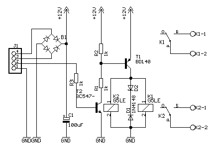
Speaker Muting
MOSFET Integrated Amp Speaker Muting
The speaker muting circuit presented here uses the MCU to
switch on the speakers after a short delay. The amount of delay can be software
programmed. At switch-off, the local supply voltage (derived from the
transformer's auxiliary 0-12 winding) collapses very quickly, switching off the
relay. The headphone jack includes a switch for speaker muting, this is sensed
by the MCU (through port RB7), which then switches off the speaker. The
circuit's input (J1.2) connects to the MCU's speaker mute relay pin (JP5.3, on
the MCU board). A logic high at this pin switches on the relay, and hence the
speakers. The relays used should have a 10A DC contact rating, otherwise serious
damage can result. The Zener diode used (ZD1) is a 12V type.
Construction
The various PCBs were built on Veroboard, excepting for the
power amplifier. These were made on FR4 PCBs, with a good ground plane, etc. The
output devices were laid flat on the board, with an aluminium L-section between
the devices and the board. This L-section is then bolted onto the
heatsink.
The amp was built into a standard amplifier case (from
Dexa). It, however, needed significant modification for this amplifier. A large
hole had to be cut in the rear to insert the heatsink. Rectangular hole was made
in the front panel to insert the LCD panel. The tape selector slots were used to
implement the menu and up/down keys. One of the other switch slots was used for
the infrared sensor. The cutouts for volume/balance/tone pots were used for
front-panel input (RCA jacks), speaker active LED and headphone socket.
Disclaimer
These circuits are provided for your own study only. They all
deal with electricity and electronics, a sufficient knowledge of both is
assumed. I will not take any responsibility for any personal injury or damage to
property arising from use or abuse of the information provided on these
pages.